- 您现在的位置:买卖IC网 > Sheet目录3890 > PIC18C858T-I/PT (Microchip Technology)IC MCU OTP 16KX16 CAN 80TQFP
2000 Microchip Technology Inc.
Advanced Information
DS30475A-page 141
PIC18CXX8
15.3
SPI Mode
The SPI mode allows 8 bits of data to be synchronously
transmitted and received, simultaneously. All four
modes of SPI are supported. To accomplish communi-
cation, typically three pins are used:
Serial Data Out (SDO) - RC5/SDO
Serial Data In (SDI) - RC4/SDI/SDA
Serial Clock (SCK) - RC3/SCK/SCL/LVOIN
Additionally, a fourth pin may be used when in any
Slave mode of operation:
Slave Select (SS) - RA5/SS/AN4
15.3.1
OPERATION
When initializing the SPI, several options need to be
specified. This is done by programming the appropriate
control bits SSPCON1<5:0> and SSPSTAT<7:6>.
These control bits allow the following to be specified:
Master mode (SCK is the clock output)
Slave mode (SCK is the clock input)
Clock polarity (Idle state of SCK)
Data input sample phase (middle or end of data
output time)
Clock edge (output data on rising/falling edge of
SCK)
Clock rate (Master mode only)
Slave Select mode (Slave mode only)
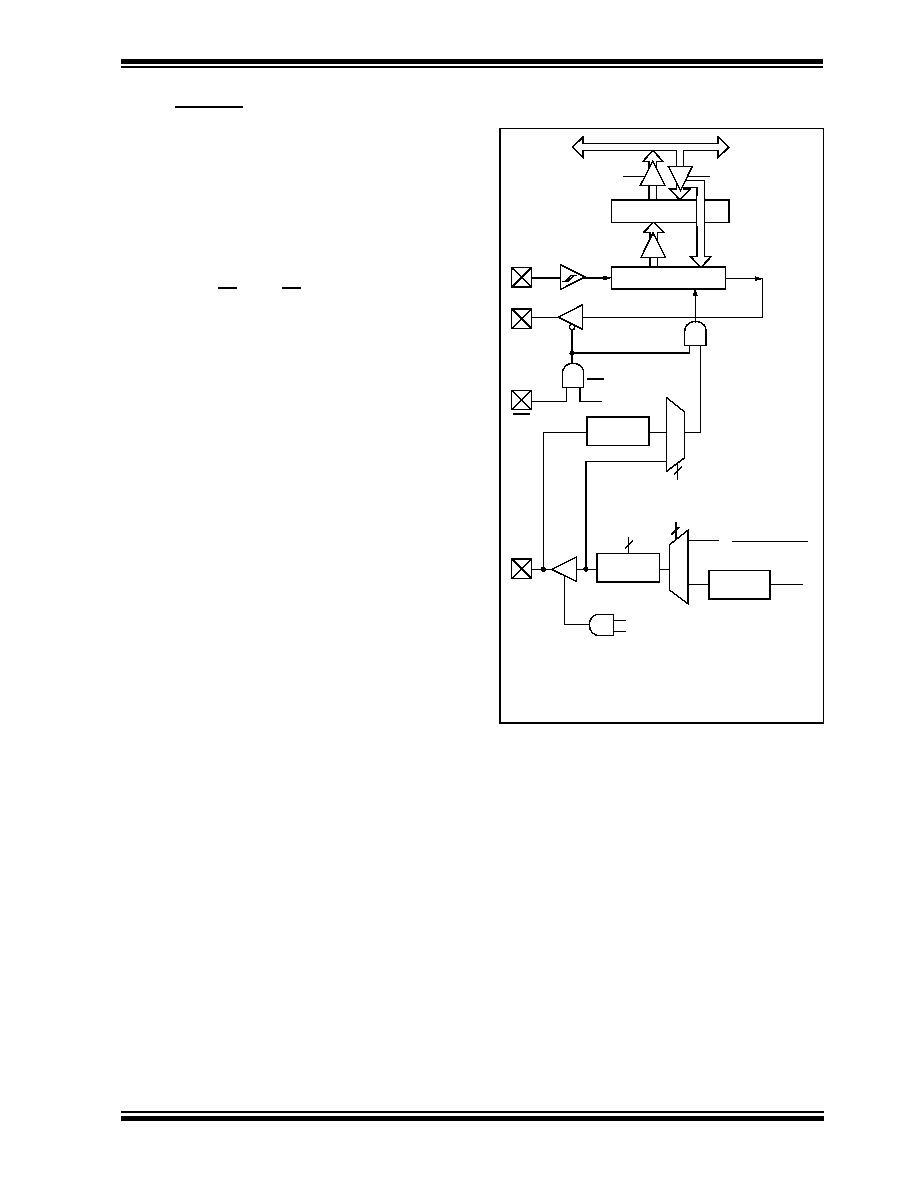
Figure 15-1 shows the block diagram of the MSSP
module, when in SPI mode.
FIGURE 15-1: MSSP BLOCK DIAGRAM
(SPI MODE)
The MSSP consists of a transmit/receive Shift Register
(SSPSR) and a buffer register (SSPBUF). The SSPSR
shifts the data in and out of the device, MSb first. The
SSPBUF holds the data that was written to the SSPSR,
until the received data is ready. Once the 8 bits of data
have been received, that byte is moved to the SSPBUF
register. Then the buffer full detect bit, BF (SSPSTAT
register), and the interrupt flag bit, SSPIF (PIR regis-
ters), are set. This double buffering of the received data
(SSPBUF) allows the next byte to start reception before
reading the data that was just received. Any write to the
SSPBUF register during transmission/reception of data
will be ignored, and the write collision detect bit, WCOL
(SSPCON1 register), will be set. User software must
clear the WCOL bit so that it can be determined if the
following write(s) to the SSPBUF register completed
successfully.
(
)
Read
Write
Internal
Data Bus
SSPSR reg
SSPM3:SSPM0
bit0
Shift
Clock
SS Control
Enable
Edge
Select
Clock Select
TMR2 Output
TOSC
Prescaler
4, 16, 64
2
Edge
Select
2
4
Data to TX/RX in SSPSR
TRIS bit
2
SMP:CKE
SDI
SDO
SS
SCK
Note:
I/O pins have diode protection to VDD and
VSS.
SSPBUF reg
发布紧急采购,3分钟左右您将得到回复。
相关PDF资料
PIC18C658T-I/PT
IC MCU OTP 16KX16 CAN 64TQFP
PIC16LC717T-E/SS
IC MCU OTP 2KX14 A/D PWM 20SSOP
PIC16LC771T/SO
IC MCU OTP 4KX14 A/D PWM 20SOIC
PIC16LC771T-E/SO
IC MCU OTP 4KX14 A/D PWM 20SOIC
PIC16C771T-E/SO
IC MCU OTP 4KX14 A/D PWM 20SOIC
PIC16LC770T/SS
IC MCU OTP 2KX14 A/D PWM 20SSOP
PIC16LC717T-I/SO
IC MCU OTP 2KX14 A/D PWM 18SOIC
PIC16LC771T/SS
IC MCU OTP 4KX14 A/D PWM 20SSOP
相关代理商/技术参数
PIC18F1220-E/ML
功能描述:8位微控制器 -MCU 4KB 256 RAM 16 I/O RoHS:否 制造商:Silicon Labs 核心:8051 处理器系列:C8051F39x 数据总线宽度:8 bit 最大时钟频率:50 MHz 程序存储器大小:16 KB 数据 RAM 大小:1 KB 片上 ADC:Yes 工作电源电压:1.8 V to 3.6 V 工作温度范围:- 40 C to + 105 C 封装 / 箱体:QFN-20 安装风格:SMD/SMT
PIC18F1220-E/P
功能描述:8位微控制器 -MCU 4KB 256 RAM 16 I/O RoHS:否 制造商:Silicon Labs 核心:8051 处理器系列:C8051F39x 数据总线宽度:8 bit 最大时钟频率:50 MHz 程序存储器大小:16 KB 数据 RAM 大小:1 KB 片上 ADC:Yes 工作电源电压:1.8 V to 3.6 V 工作温度范围:- 40 C to + 105 C 封装 / 箱体:QFN-20 安装风格:SMD/SMT
PIC18F1220-E/SO
功能描述:8位微控制器 -MCU 4KB 256 RAM 16 I/O RoHS:否 制造商:Silicon Labs 核心:8051 处理器系列:C8051F39x 数据总线宽度:8 bit 最大时钟频率:50 MHz 程序存储器大小:16 KB 数据 RAM 大小:1 KB 片上 ADC:Yes 工作电源电压:1.8 V to 3.6 V 工作温度范围:- 40 C to + 105 C 封装 / 箱体:QFN-20 安装风格:SMD/SMT
PIC18F1220-E/SS
功能描述:8位微控制器 -MCU 4KB 256 RAM 16 I/O RoHS:否 制造商:Silicon Labs 核心:8051 处理器系列:C8051F39x 数据总线宽度:8 bit 最大时钟频率:50 MHz 程序存储器大小:16 KB 数据 RAM 大小:1 KB 片上 ADC:Yes 工作电源电压:1.8 V to 3.6 V 工作温度范围:- 40 C to + 105 C 封装 / 箱体:QFN-20 安装风格:SMD/SMT
PIC18F1220-H/ML
功能描述:8位微控制器 -MCU 4KB FL 256RAM 16 I/O RoHS:否 制造商:Silicon Labs 核心:8051 处理器系列:C8051F39x 数据总线宽度:8 bit 最大时钟频率:50 MHz 程序存储器大小:16 KB 数据 RAM 大小:1 KB 片上 ADC:Yes 工作电源电压:1.8 V to 3.6 V 工作温度范围:- 40 C to + 105 C 封装 / 箱体:QFN-20 安装风格:SMD/SMT
PIC18F1220-H/P
功能描述:8位微控制器 -MCU 4KB FL 256RAM 16 I/O RoHS:否 制造商:Silicon Labs 核心:8051 处理器系列:C8051F39x 数据总线宽度:8 bit 最大时钟频率:50 MHz 程序存储器大小:16 KB 数据 RAM 大小:1 KB 片上 ADC:Yes 工作电源电压:1.8 V to 3.6 V 工作温度范围:- 40 C to + 105 C 封装 / 箱体:QFN-20 安装风格:SMD/SMT
PIC18F1220-H/SO
功能描述:8位微控制器 -MCU 4KB FL 256RAM 16 I/O RoHS:否 制造商:Silicon Labs 核心:8051 处理器系列:C8051F39x 数据总线宽度:8 bit 最大时钟频率:50 MHz 程序存储器大小:16 KB 数据 RAM 大小:1 KB 片上 ADC:Yes 工作电源电压:1.8 V to 3.6 V 工作温度范围:- 40 C to + 105 C 封装 / 箱体:QFN-20 安装风格:SMD/SMT
PIC18F1220-H/SS
功能描述:8位微控制器 -MCU 4KB FL 256RAM 16 I/O RoHS:否 制造商:Silicon Labs 核心:8051 处理器系列:C8051F39x 数据总线宽度:8 bit 最大时钟频率:50 MHz 程序存储器大小:16 KB 数据 RAM 大小:1 KB 片上 ADC:Yes 工作电源电压:1.8 V to 3.6 V 工作温度范围:- 40 C to + 105 C 封装 / 箱体:QFN-20 安装风格:SMD/SMT